



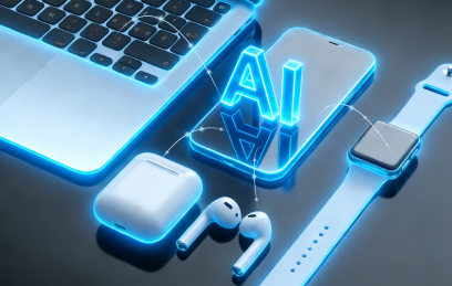
AI Smart Terminal Solution
With the advancement of AI smartphones and other terminal products, increasingly complex structure, and miniaturized features such as holes, circuit, and dielectric thickness.
Mainstream smartphones adopt high-end HDI boards; while high-end models adopt anylayer HDI or substrate-like PCBs. Typical manufacturing processes include the subtractive process (Tenting L/S ≥ 35/35 μm) and the modified semi-additive process (mSAP L/S ≤ 30/30 μm). Next-generation smartphone motherboards are shifting from traditional FR-4 materials to RCC and ABF, meet higher-density wiring needs. In addition, flexible printed circuits (FPCs) serve as critical 3D interconnection inside smart device supports more functions, with multi-layer design and high density as the main development trend.
In response to the technological trends in the smartphone industry, Han's CNC provides diversified product solutions to empower the industrial technological upgrading.

They are all partnering with us.
We serve leading PCB enterprises worldwide, covering the top 100 PCB manufacturers in China, and gaining customer recognition with technology and quality.







Ranking is not in any particular order